Memory
Where the temporary data and instructions of currently running programs are located. Computer memory also known as Primary Memory.
Two main types of memory: - Cache - Random Access Memory (RAM)
Cache
Cache located within the CPU itself and hence is extremely fast compared to RAM, as it runs at the same clock speed as the CPU. Very limited in size and very sophisticated, expensive to manufacture due to it being so close to the CPU core.
Main benegit of cache memory, enabling the CPU to access upcoming instructions and data quicker than retrieving them from RAM.
Three levels of cache:
Level 1 Cache= Usually in kilobytes, the fastest memory available, located in each CPU coreLevel 2 Cache= Usually in megabytes, extremely fast (slower than L1), dedicated to each CPU core, serves as a middle tier between L1 and L3Level 3 Cache= Usually in megabytes (larger than L2), faster than RAM slower than L1/L2
RAM
Much larger than cache and accessing data from RAM takes many more instructions!
Example: retrieving an instruction from the registers takes only one clock cycle, and retrieving it from the L1 cache takes a few cycles, while retrieving it from RAM takes around 200 cycles…
Maximum possible RAM was 2^32 bytes for 32 bit OS, which is only 4 GB
at which point we run out of unique address. With 64-bit, range is now
up to 0xffffffffffffffff, theoretical max of 2^64 ->
18.5 exabytes (18.5 million terabytes)
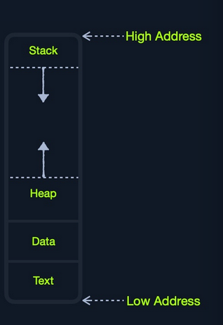
RAM is split into four main segments:
- Stack = Last-In, First-out (LIFO) design and is fixed in size. Data in it can only be accessed in a specific order by push-ing and pop-ing data
- Heap = Hierarchical design and much larger and more versatile in storing data, as data can be stored retrieved in any order. Heap slower than the Stack
- Data = Has two parts:
Data, which is used to hold variables, and.bss, which is used to hold unassigned variables (buffer memory for later allocation) - Text = Main assembly instructions are loaded into this segment to be fetched and executed by the CPU
IO/Storage
Input/Output devices like keyboards, screen, or long-term storage
unit. Processor can access and control IO devices using
Bus Interfaces, acting as ‘highways’ to transfer data and
addresses, using electrical charges for binary data.
Each bus has a capacity of bits (or electrical charges) it can carry simultaneously. Usually a multiple of 4-bits, ranging up to 128-bits. Bus interfaces are also usually used to access memory and other components outside the CPU itself. (Think about the PCB lanes on a board, those are the bus lines.
CPU Architecture
CPU contains both Control Unit (CU) -> in charge of
moving and controlling data Arithmetic/Logic Unit (ALU)
-> in charge of performing various arithmetics and logical
calculations as requested by a program through the assembly
instructions.
Instruction Set Architecture (ISA) -> different ways
that a CPU processes its instructions, can can also influence how
efficiently the CPU processes instructions as well. Basically why ARM
binaries don’t run on x86 arch computers, vice versa.
Example writting the same instruction on different ISAs:
add rax, 1is for Intel x86 64-bit processorsadd r1, r1, 1is for ARM processors
A single ISA may have several syntax interpretations for the same
assembly code (Intel syntax add rax, 1
vs. addb $0x1,%rax AT&T syntax)
RISC -> based on processing more simple instructions,
taking more cycles, but each one shorter and taking less power
CISC -> based on fewer cycles, but each instruction
taking more time and power to be processed
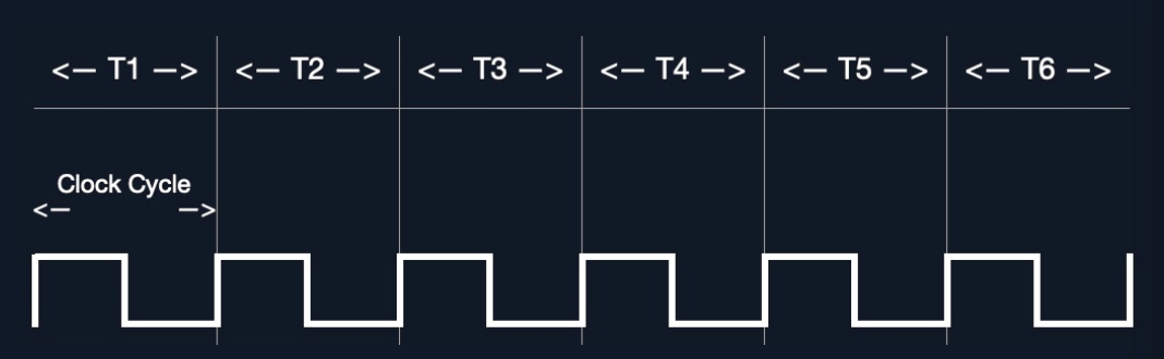
Clock Speed & Clock Cycle
Each CPU has a clock speed to indicate overall speed. Every tick of
clock runs a clock cycle that processes a basic instruction, like
fetching an address or storing an address. This is done by the
CU or ALU
Frequency in which cycles occur is counted is cycles per second
(Hertz, Hz). Ex: If CPU has speed of 3.0 GHz,
that means it can run 3 billion cycles every second (per core).
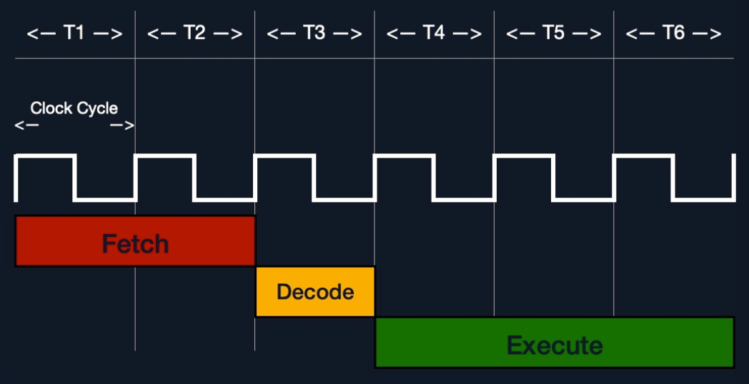
Instruction Cycle
Instruction Cycle -> cycle it take the CPU to process
a single machine instruction
Four stages:
Fetch-> take the next instruction’s address from theInstruction Address Register (IAR)that tells it where the next instruction is locatedDecode-> take instruction from the IAR and decode it from binary to see what is required to executedExecute-> Fetch instruction operands from register/memory, and process the instruction in theALUorCUStore-> Store the new value in the destination operand
All stages in the instruction cycle are carried out by the
CU, but arithmetic instruction like “add, sub, etc.” are
executed by the ALU
Ex with add rax, 1, this is the instruction cycle:
- Fetch instruction from the
ripregister,48 83 C0 01 - Decode
48 83 C0 01to know it needs to perform anaddof1to value atrax - Get the current value at
rax(by theCU), add1to it (by theALU) - Store the new value back to
rax
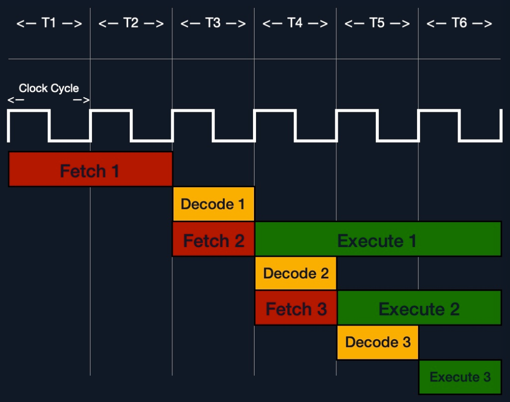
Above is executing process instructions sequentially as it was done in the past. With modern multi-thread and multi-core design CPUs, processors can process multiple instructions in parallby having multiple instruction/clock cycles running at the same time.
TIP: If we want to know what architecture the system supports use
lscpu - can also use uname -m to get CPU
architecture.
Instruction Set Architecutres
Instruction Set Architecture (ISA) specifies the syntax
and semantics of assembly language on each architecture. Not just
different syntax, but afffects the way and order instructions are
executed and the level of complexity
ISA consists of:
- Instructions
- Registers
- Memory Addresses
- Data Types
And there are two main ISA widely used:
Complex Instruction Set Computer-> Intel and AMD processors in most computers and serversReduced Instruction Set Computer-> Used in ARM and Apple processors, in most smartphones and some modern laptops
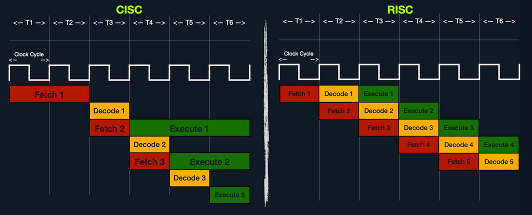
CISC vs RISC
- CISC favors complex instructions, RISC favors simple instructions
- Longer instructions, variable length, multiples of 8-bits, Shorter instr, fixed length 32 or 64 bit
- Fewer total instructions (shorter code), More total instructions (longer code)
- Relies on hardware optimization of CPU, Relies on software optimization in assembly
- Instruction Execution Time is variable, multiple clock cycles, where RISC is fixed, one clock cycle
- Instructions supported by CPU is many (~1500), fewer instructions (~200)
- power comsumption is high vs. very low
Registers, Addresses, and Data Types
Registers
Each CPU core has a set of registers, they are the fastest components in any computer close to the CPU core.
Two main types of registers to focus on: Data Registers
and Pointer Registers
| Data Registers | Pointer Registers |
|---|---|
| rax | rbp |
| rbx | rsp |
| rcx | rip |
| rdx | |
| r8 | |
| r9 | |
| r10 |
Data Registers- used for storing instructions/syscall arguments.Pointer Registers- used to store specific important address- Main pointer registers are the Base Stack Pointer
rbp, points to the beginning of the Stack - Current Stack Point
rsp-> points to the current location within the Stack (top of the Stack) - Instruction Pointer
rip-> holds the address of the next instruction
Sub-Registers
64-bit register can be divided into smaller
sub-registers, one byte 8-bits, 2 bytes
16-bits, and 4 bytes32-bits`

| Size in bits | Size in bytes | Name | Example |
|---|---|---|---|
16-bit |
2 bytes |
the base name | ax |
8-bit |
1 bytes |
base name and/or ends with l |
al |
32-bit |
4 bytes |
base name + starts with the e prefix |
eax |
64-bit |
8 bytes |
base name + starts with the r prefix |
raw |
| Description | 64-bit Register | 32-bit Register | 16-bit Register | 8-bit Register |
|---|---|---|---|---|
| Data/Arguments Registers | ||||
| Syscall Number/Return value | rax |
eax |
ax |
al |
| Callee Saved | rbx |
ebx |
bx |
bl |
| 1st arg - Destination operand | rdi |
edi |
di |
dil |
| 2nd arg - Source operand | rsi |
esi |
si |
sil |
| 3rd arg | rdx |
edx |
dx |
dl |
| 4th arg - Loop counter | rcx |
ecx |
cx |
cl |
| 5th arg | r8 |
r8d |
r8w |
r8b |
| 6th arg | r9 |
r9d |
r9w |
r9b |
| Pointer Registers | ||||
| Base Stack Pointer | rbp |
ebp |
bp |
bpl |
| Current/Top Stack Pointer | rsp |
esp |
sp |
spl |
| Instruction Pointer ‘call only’ | rip |
eip |
ip |
ipl |
Note: there are various other registers like
RFLAGSregister, used to maintain various flags used by the CPU, like the zero flagZFused for conditional instructions
Memory Addresses
RAM is segmented into various regions like the Stack, heap, and other kernel-specific regions.
Each memory region has specific read,
write,execute` permissions that specify if you can read
from it, write to it, or call an address in it.
When a instruction goes through the Instruction Cycle to be executed, first step is to fetch the instruction from the address it’s located at.
Different types of address fetching (i.e. addressing modes) in x86:
| Addressing Mode | Description | Example |
|---|---|---|
Immediate |
value is given within the instruction | add 2 |
Register |
register name that holds the value is given in the instruction | add rax |
Direct |
direct full address is given in the instruction | call 0xfffffffffaa8a25ff |
Indirect |
reference pointer is given in the instruction | call 0x44d000 or call [rax] |
Stack |
address is on top of the stack | add rsp |
In the table above, lower is slower. The less immediate the value is, the slower it is to fetch it.
Speed isn’t the biggest concern when learning Assembly, but understand where and how each address is located - helps in binary exploitation like Buffer Overflows. Same understanding will have an even more significant implication with advanced binary exploitation, like ROP or Heap exploitation.
Address Endianness
This is the order of its bytes in which they are stored or retrieved from memory. Two types:
Little-Endian= little-end byte of the address is filled/retrieved first right-to-leftBig-Endian= big-end byte of the address is filled/retrieved first left-to-right
For address 0x0011223344556677 to be stored in memory,
little-endian procesors would store 0x00, then
0x1100, then 0x221100, until all of them are
in place it would look like 0x7766554433221100
Another example to show how this can affect stored values in binary.
For a 2-byte integer 426, its binary representation is
00000001 10101010, value becomes 43521.
Big-endian processors would store these bytes as
00000001 10101010 (left-to-right), while
little-endian processors store them as 10101010 00000001
(right-to-left).
When we retrieve the value, the processor has to use the same endianness used when storing them, or it will get the wrong value. This indicates that the order in which the bytes are stored/retrieved make a big difference
For this course, we’ll be using little-endian order, which is used with Intel/AMD x86 modern operating systems.
The bytes we will be storing into memory from right-to-left
- FOR EXAMPLE: to push an address or string with Assembly, we would
push it in reverse. Like storing the word
Hello, we would push its bytes in reverse:o,l,l,e, andH.
Seems counter-intuitive since people are used to reading from left-to-right. But there are multiple advantages when processing data, like being able to retrieve a sub-register without having to go through the entire register or being able to perform arithmetic in the correct order right-to-left.
Data Types
x86 arch supports many types of data sizes, which can be used with various instructions. Here are the most common data types:
| Component | Legth | Example |
|---|---|---|
byte |
8 bits | 0xab |
word |
16 bits - 2 bytes | 0xabcd |
double word (dword) |
32 bits - 4 bytes | 0xabcdef12 |
quad word (qword) |
64 bits - 8 bytes | 0xabcdef1234567890 |
Whenever we use a variable with a certain data type or use a data type with an instruction, both operands should be of the same size!
Example: can’t use a variable defined as byte with
rax, since rax is 8 bytes. We would have to
use al, which is 1 byte.
| Sub-register | Data Type |
|---|---|
al |
byte |
ax |
word |
eax |
dword |
rax |
qword |
Assembly File Structure
We need to first understand the general structure of an assembly file and then how to assemble it and debug it.
         global  _start

         section .data
message: db      "Hello HTB Academy!"

         section .text
_start:
         mov     rax, 1
         mov     rdi, 1
         mov     rsi, message
         mov     rdx, 18
         syscall

         mov     rax, 60
         mov     rdi, 0
         syscall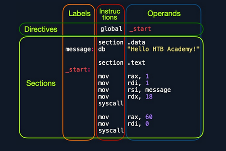
Looking at the vertical parts of code, each line can have three elements
| 1. Labels | 2. Instructions | 3. Operands |
|---|
A label can be referred to by instructions
or by directives
| Section | Description |
|---|---|
global _start |
This is a directive that directs the code to start
executing at the _start_ label defined below. |
section .data |
The data section, which should contain all of the
variables. |
section .text |
The text section containing all of the code to be
executed. |
References
- {Source}